Feb 17, 2017

High-resolution OLED microdisplay for virtual reality applications

Test and qualification vehicle of the LOMID chip with a screen diagonal of 2.5 cm and a resolution of 1920 × 1200 (WUXGA).
Source: Fraunhofer FEP, Jürgen Lösel
Feb 17, 2017
With applications ranging from gaming to assembly, maintenance information supply, and pilot training in flight simulators, virtual reality glasses and their supporting systems are becoming more and more established, whilst at the same time also initiating and facilitating developments in new fields. A crucial aspect of virtual reality presentations is the display technology. Here, OLED microdisplays are receiving growing attention due to their technological advantages. 
 
The Fraunhofer FEP has long-term experience and a vast knowledge of the development and fabrication of customized OLED microdisplays for various applications. Within the EU-funded H2020 project LOMID (Large cost-effective OLED microdisplays and their applications), which is led by scientists at the Fraunhofer FEP, a new generation of large area OLED microdisplays has been developed which focusses on both virtual-reality (VR) and augmented-reality (AR, the latter will be tested within the project in visual prosthetics). In the LOMID project, flexible OLED microdisplays of exceptionally large area (13 mm × 21 mm) with a screen diagonal of 24.9 mm (~1”) will be manufactured at challenging high yields (>60%). This will be achieved by developing a robust silicon-based chip design enabling both high resolution (1200×1920 (WUXGA) with pixel sizes of 11 μm × 11 μm for a pixel density of 2300 ppi) and highly reliable manufacturing of the backplane. 
 
Mike Thieme, project manager at LOMID contributor X-FAB, says: “Economical processes (e.g. based on 0.18 and 0.35 μm lithography) are being developed at the CMOS silicon foundry and special attention will be given to the interface between the top metal electrode of the CMOS backplane and the subsequent OLED layers. In order to keep the CMOS manufacturing at low cost, numerous design rules have been pushed to their limits.”
 
Additional challenges such as conformability of the OLED microdisplays will be addressed to allow a bending radius of 50 mm. Along with these new functionalities, the durability of the devices when bent has to be guaranteed and be comparable to that of rigid devices. This will be addressed by improving the OLED robustness and by modifying the device encapsulation to simultaneously fulfill stringent barrier requirements (WVTR < 10-6 g/d m2) and to provide sufficient mechanical protection.

The high interest in large area microdisplays is demonstrated by the strong participation of industrial partners. The project will run until 31.12.2017 and will provide a high-performance OLED microdisplay with new functionalities addressing a wider range of applications.
 
Contact: Ines Schedwill, Fraunhofer Institute for Organic Electronics, Electron Beam and Plasma Technology FEP
Ines.Schedwill@fep.fraunhofer.de

Recommended articles

Aug 16, 2023

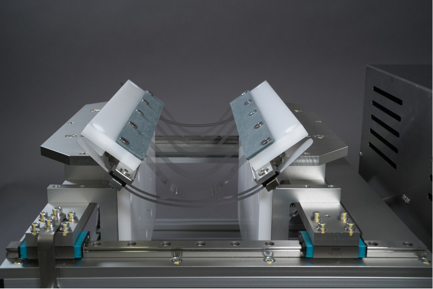
For more than ten years, Fraunhofer FEP has been involved in the processing of ultra-thin glass, especially in the handling …

Dec 1, 2022

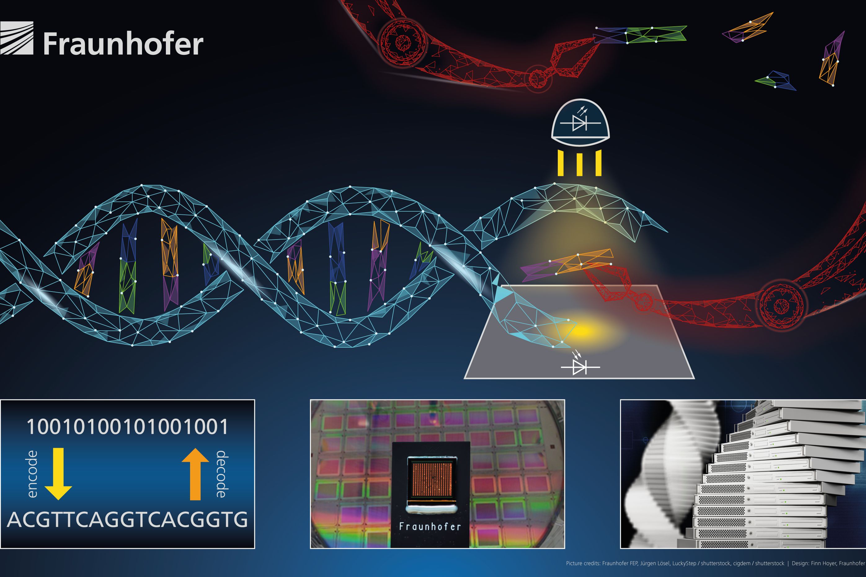
DNA is not only the basic medium for storing genomic information, but can also be used to store binary data. …

Nov 25, 2022

The internet of tomorrow will be mobile and audio based. To support the shift in communication from typing and reading …

Recommended events

Mar 5 - 7, 2025
Discover the Future of Photonics with IVAM
Feb 4 - 6, 2025
Medical Design & Manufacturing - IVAM presents Micro Nanotech Area in Hall C
Nov 11 - 14, 2024
Product Market “High-tech for Medical Devices” and "COMPAMED HIGH-TECH FORUM" in Hall 8a, F29 (IVAM Lounge)